PCB Etching Process: Understanding the Different Techniques and Their ImpactAuthor : Adrian September 04, 2025Table of ContentsAre you looking to understand the PCB etching processand how it impacts the quality and precision of printed circuit boards? In simple terms, PCB etching is a critical step in PCB manufacturingwhere unwanted copper is removed from the board to create the desired circuit pattern. There are various techniques like chemical etching PCB, wet etching, and dry etching, each with unique benefits, challenges, and effects on etching tolerances. In this comprehensive guide, we’ll break down these methods, explore their impact on manufacturing, and provide actionable insights to help you choose the right approach for your project.
What Is the PCB Etching Process?The PCB etching processis a fundamental part of creating printed circuit boards. It involves removing excess copper from a copper-clad board to form the conductive traces and pads that make up the circuit design. This process is essential for transforming a blank board into a functional component used in electronics, from smartphones to industrial machinery. Etching can be performed using different techniques, each suited to specific applications based on factors like precision, cost, and production volume. The most common methods include chemical etching PCB(often referred to as wet etching), dry etching, and emerging technologies like laser etching. Understanding these techniques helps engineers and manufacturers achieve the desired etching tolerancesand ensure high-quality results in PCB manufacturing.
Why Is PCB Etching Important?Etching directly affects the performance and reliability of a printed circuit board. If done incorrectly, it can lead to issues like over-etching, where too much copper is removed, causing weak traces or open circuits. Under-etching, on the other hand, leaves excess copper, which can result in short circuits. Achieving precise etching tolerances—often within a range of ±10% of the trace width (e.g., ±0.001 inches for a 0.010-inch trace)—is crucial for maintaining signal integrity, especially in high-frequency applications where impedance control is critical (typically targeting 50 ohms for RF designs). Beyond functionality, the choice of etching technique impacts production costs, turnaround times, and environmental considerations. Let’s dive into the different methods to see how they work and where they fit best in PCB manufacturing.
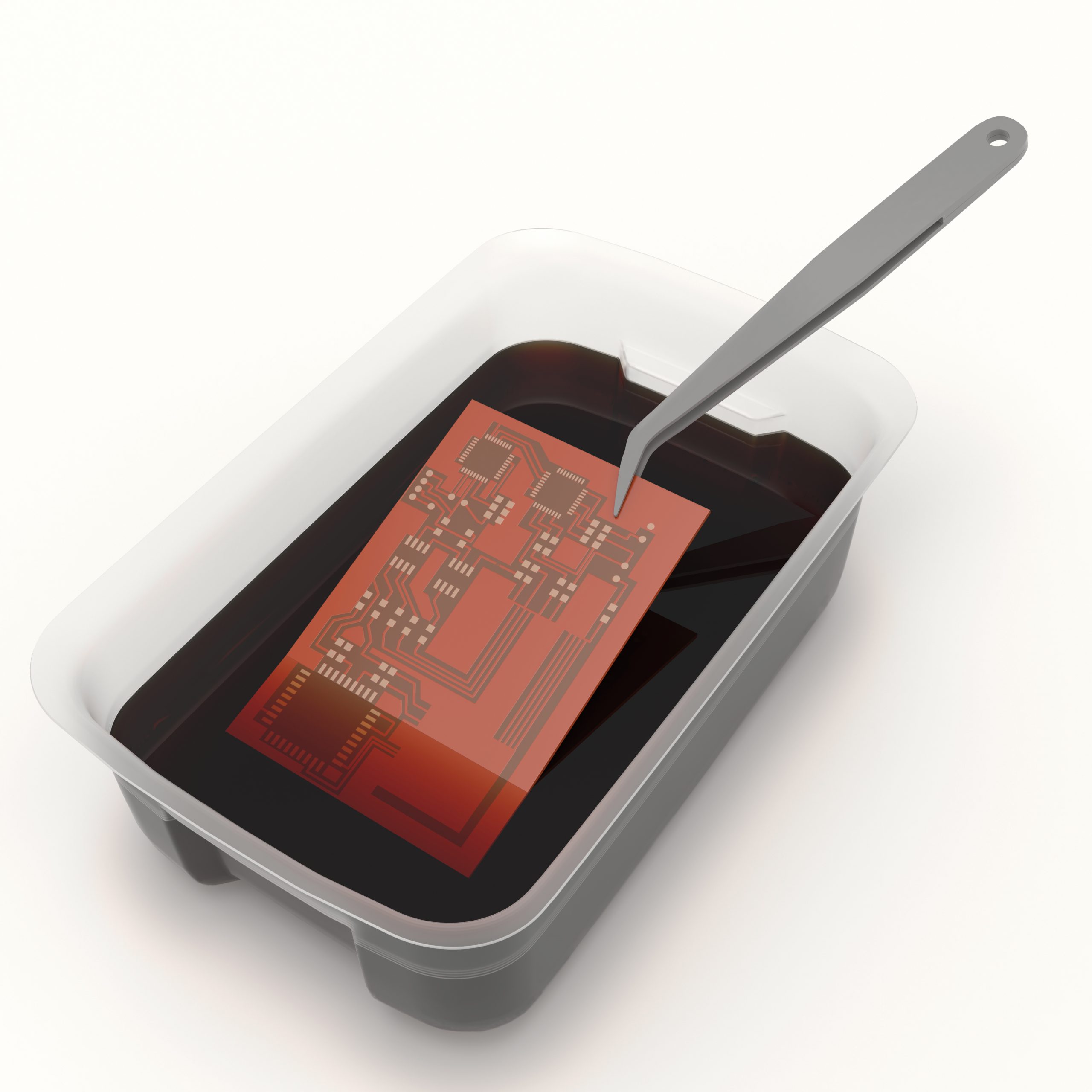
Types of PCB Etching Techniques1. Chemical Etching PCB (Wet Etching)Wet etching, also known as chemical etching PCB, is the most traditional and widely used method in PCB manufacturing. In this process, the board is immersed in a chemical solution that dissolves the unprotected copper, leaving behind the circuit pattern protected by a resist layer (often a photoresist or etch-resistant ink). How It Works:
Advantages:
Challenges:
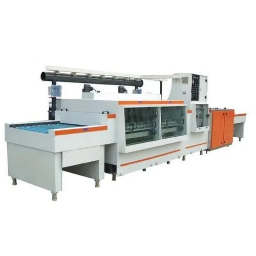
2. Dry EtchingDry etchingis a more advanced technique often used in high-precision PCB manufacturing, especially for complex, high-density interconnect (HDI) boards. Unlike wet etching, dry etching uses plasma or gaseous etchants to remove copper or other materials without liquid chemicals. How It Works:
Advantages:
Challenges:
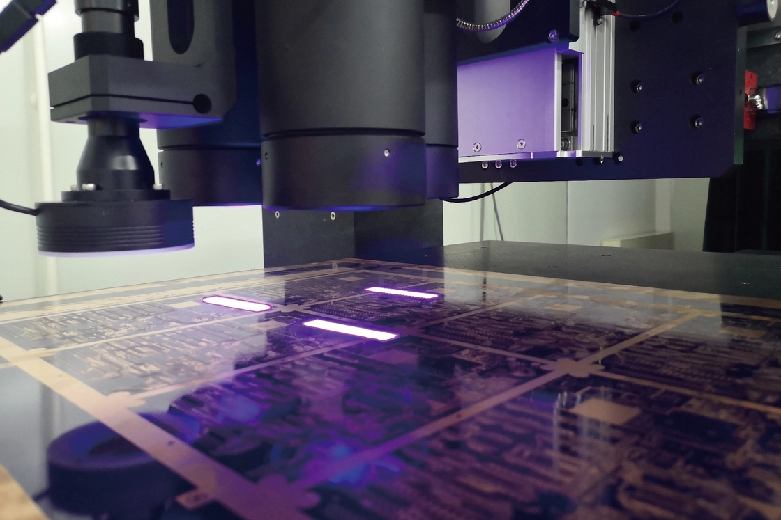
3. Laser EtchingLaser etching is an emerging method in the PCB etching process, using focused laser beams to remove copper or other materials with extreme precision. While not as common as wet or dry etching, it’s gaining traction for specialized applications. How It Works:
Advantages:
Challenges:
Etching Tolerances: Why Precision Matters in PCB ManufacturingIn PCB manufacturing, etching tolerancesrefer to the acceptable deviation in trace width, spacing, and other dimensions after the etching process. These tolerances are critical because even small variations can impact the board’s electrical performance, especially in high-speed or high-frequency applications. For example, a trace width designed to be 0.008 inches with a tolerance of ±0.001 inches ensures the impedance remains within the target range (e.g., 50 ohms for differential pairs in USB or HDMI designs). If the etching process exceeds this tolerance due to undercutting or uneven etching, signal integrity issues like crosstalk or signal delay can occur, with delays potentially increasing by 10-20 picoseconds per inch of trace length. Different etching methods offer varying levels of control over tolerances:
Choosing the right etching technique depends on the design requirements, such as trace density, board complexity, and performance expectations. For instance, a simple power supply board may work fine with wet etching, while a 5G communication board demands the precision of dry or laser etching.
Factors Affecting the PCB Etching ProcessSeveral factors influence the outcome of the PCB etching process, regardless of the technique used. Understanding these can help optimize results and minimize defects. 1. Etchant Type and ConcentrationIn wet etching, the type and concentration of the chemical solution significantly affect the etch rate and uniformity. For instance, ferric chloride etches at a rate of approximately 0.001 inches per minute at 40°C, while higher concentrations or temperatures can double this rate but risk over-etching. 2. Temperature and AgitationHigher temperatures and agitation (stirring the etchant) speed up the etching process in wet methods but must be controlled to avoid uneven results. A temperature range of 35-50°C is often optimal for most chemical etchants. 3. Resist QualityThe quality and thickness of the resist layer determine how well the desired copper areas are protected. A poorly applied resist can lead to defects like pinholes, causing unintended copper removal. 4. Board Material and Copper ThicknessStandard FR-4 boards with 1 oz copper (35 microns) etch faster than thicker 2 oz copper (70 microns) layers. Thicker copper requires longer exposure to etchants or more aggressive methods, impacting production time.
Environmental and Safety Considerations in PCB EtchingThe PCB etching process, particularly chemical etching PCB, raises environmental and safety concerns due to the use of hazardous materials. Wet etching chemicals like ferric chloride are toxic and require proper handling and disposal to prevent contamination. Modern PCB manufacturingfacilities often implement recycling systems or use less harmful etchants like sodium persulfate to reduce environmental impact. In contrast, dry etchingand laser etching produce minimal chemical waste, making them more sustainable options. However, the high energy consumption of dry etching equipment and laser systems can offset some of these benefits. Balancing performance, cost, and environmental responsibility is a growing focus in the industry.
Choosing the Right Etching Technique for Your ProjectSelecting the best etching method for your PCB project depends on several factors:
By aligning the etching method with your project’s specific needs, you can optimize both quality and cost-efficiency in PCB manufacturing.
Conclusion: Mastering the PCB Etching Process for Better ResultsThe PCB etching processis a cornerstone of PCB manufacturing, shaping the functionality and reliability of every printed circuit board. Whether you choose chemical etching PCBthrough wet etchingfor its affordability, dry etchingfor its precision, or laser etching for cutting-edge applications, understanding the strengths and limitations of each technique is key to achieving the desired etching tolerancesand performance. By considering factors like design requirements, production scale, and environmental impact, you can make informed decisions that enhance the quality of your PCBs. At ALLPCB, we’re committed to supporting your projects with expert guidance and state-of-the-art manufacturing solutions tailored to your needs. Dive into the world of PCB etching with confidence, knowing you have the knowledge to create high-performing, reliable boards for any application.
 The Role of Flux in PCB Wave Soldering: Selection, Application, and Residue RemovalMarch 16, 2026PCB wave soldering flux types include rosin, water-soluble, and no-clean options with varying activity levels for oxide removal and solder flow. This guide covers selection criteria, spray foam drop-jet application methods, residue removal processes, and alternatives like nitrogen blanketing to boost joint reliability and yields for engineers. Article Achieving Uniform Solder Fillets in PCB Wave Soldering: Process ControlMarch 16, 2026Achieve uniform solder fillets in PCB wave soldering with process control strategies. Optimize flux, preheat, wave height, conveyor speed for consistent fillet shape, height, and wetting balance. Includes visual inspection tips and troubleshooting for reliable through-hole assemblies. Boost quality in production. Article Optimizing Conveyor Speed for Efficient PCB Wave SolderingMarch 16, 2026Learn PCB wave soldering conveyor speed calculation to manage dwell time, immersion depth, and throughput effectively. Electric engineers get practical steps, best practices, and troubleshooting tips for higher process efficiency and fewer defects in wave soldering operations. Article Understanding IPC Standards for PCB Surface Finishes: Ensuring Quality and ComplianceMarch 11, 2026Understand IPC standards IPC 4552 ENIG and IPC 4553 immersion silver for PCB surface finishes. Ensure compliance, enhance solderability, and prevent common defects to achieve reliable, high quality circuit boards. Article Miniaturization Challenges in PCB AssemblyMarch 11, 2026Navigate the complexities of high density interconnect PCB assembly and precise component placement. Learn to tackle miniaturization challenges, from tiny part handling to thermal stress, ensuring robust and reliable electronics. Article High Speed Routing Techniques: PCBMarch 11, 2026Master high speed routing in PCBs to ensure signal integrity and minimize electromagnetic interference. Learn essential techniques for robust designs, from controlled impedance to differential pair strategies. Prevent performance issues and achieve reliable electronics. ArticleGet Instant PCB |